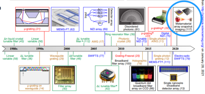
2021年1月29日,国际顶级期刊Science发表综述论文Miniaturization of optical spectrometers(光学光谱仪的小型化),将清华大学快照式CMOS超光谱成像芯片技术列为该领域最新研究成果,与光科技的使命就是实现该成果的产业化和应用落地。

过去十年,微型光谱仪发展活跃,2017年美国消费电子展(CES)上的展示和近年来主流手机制造商的专利申请情况表明,光谱传感系统嵌入智能手机的应用即将实现。适用于智能手机的应用前景,是促使微型光谱仪的兴起和发展的重要因素之一,这一领域也获得行业和投资方的高度关注。同时,计算光谱仪也成为了其中最具有发展前景的研究方向。在实现瞬时捕捉光谱和空间信息的高光谱成像应用基础上,这一方向的长期目标就是实现具有高光谱和空间分辨率的小型、便携、快照式光谱成像仪,即每个像素都相当于一个高性能光谱仪。这种系统将是当前研究中一个里程碑式的提升,当前光谱成像技术一般都涉及到可移动的扫描系统或基于数字镜设备的空间光调制器。随着计算光谱仪的有效感知区域缩小至10μm的量级,这种高光谱成像系统越来越具有可行性。文中提及的清华大学快照式CMOS超光谱成像芯片技术(117),将“超像素”(superpixels)阵列集成到一个CMOS图像传感器上,每个“超像素”相当于一个微型光谱仪,都具有独立的光谱分析功能。(编译自原文)
清华大学快照式CMOS超光谱成像芯片技术是微纳光电子学实验室10余年积累的成果,由黄翊东教授课题组的崔开宇副教授提出并研制。该芯片成功实现CMOS集成,一次拍照即可获得一幅完整的光谱图像,即可以一次获得空间上不同点的光谱信息,每个微型光谱仪都具有独立的光谱分析功能。这些单个微型光谱仪的技术指标(如光谱分辨率)已超过国际上报道的最好结果,而集成的快照式超光谱成像芯片则是在公开论文中的首次报道。该光谱成像芯片可以利用成熟的半导体工艺制程实现制造,是可量产的硅基微型光谱成像方案,实现了从微型光谱仪到光谱成像芯片的跨越。该技术由与光科技进行产业化和应用落地。
与光科技致力于成为全球光谱芯片的引领者,让光谱感知无处不在。与光科技由长江学者特聘教授领衔,创新性地研发了快照式CMOS超光谱成像芯片,该芯片具有精度高、成本低、可量产的优势,打破了现有光谱检测设备体积庞大、价格高昂、仅支持扫描式成像的瓶颈,将为消费电子、医疗诊断、机器视觉、环保监测等行业拓展新的传感维度。
“More recently, the development of spectral sensing systems embedded within smartphones has been evidenced, at CES (consumer electronics show) 2017 and in patent applications by major smartphone manufacturers, suggesting that an emergence into the public domain may be imminent. Indeed, the prospect of a device with a footprint suitable for the smartphone paradigm is arguably the most important factor driving extreme miniaturization of microspectrometer systems; a breakthrough demonstration here could prove pivotal in terms of attracting further attention and investment in this field. Although no reconstructive systems have reached commercial maturity as yet, the readily available processing power, coupled with the need for systems with minimized footprint and weight, make the smartphone platform an obvious area for these microspectrometers to emerge.”
“Perhaps most exciting are the possibilities for hyperspectral imaging applications involving the simultaneous capture of spectral and spatial information in a “data cube” with dimensions (x, y, λ). Here a long-term goal is a miniaturized, portable “snapshot” spectral imager with high spectral and spatial resolution—that is, a camera whereby each pixel holds its own high-performance spectrometer. Such a system would be a marked advance on many current strategies in development, which involve scanning systems with movable parts, or digital mirror device–based spatial light modulators (116). Given their simple (and usually planar) device frameworks, as the active sensing area of computational microspectrometers shrinks toward the ~10 μm scale, miniaturized snapshot imagers based on such concepts become increasingly feasible. Indeed, successful prototypes based on arrays of “superpixels,” each containing their own filter array, have very recently been reported (117, 118). ”


